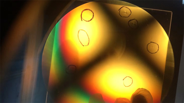
The main application areas of silicon carbide wafers are LED solid state lighting and high frequency devices. The material has excellent characteristics such as band gap, drift velocity, breakdown voltage, thermal conductivity and high temperature resistance which are several times higher than those of traditional silicon, and has irreplaceable advantages in electronic application fields such as high temperature, high voltage, high frequency, high power, photoelectricity, radiation resistance, microwave and extreme environment applications such as aerospace, military industry and nuclear energy. The exclusive supplier of silicon carbide single crystal in China is in the absolute leading position in research and development, technology, market development and commercial operation, and has successfully mastered the core technology of 76mm (3 inches) super-large gem-grade SiC2 crystal growth, reaching the international advanced level in 2001.
In the application of semiconductor devices, with the reduction of the production cost of silicon carbide, silicon carbide may replace silicon as a chip because of its excellent performance, which will break the bottleneck of the material performance of silicon chips and bring revolutionary changes to the electronic industry. The main application fields of silicon carbide are LED solid state lighting and high frequency devices. In the future, the background light market of mobile phones and notebook computers will provide huge demand growth for silicon carbide.
The polarized stress meter independently developed and produced by Suzhou PTC Optical Instrument Co., Ltd. can be used to detect defects of silicon carbide wafers, such as scratches, bubbles, dirt, etc.
