Various electronic devices commonly found in daily life, such as mobile phones, computers, TVs, and air conditioners, all rely on the logical calculation, storage, and sensing capabilities provided by various chips.
The core of each chip is a die, which is cut from a variety of wafers. The wafer itself has yield problems, and various defects may exist on the surface of the wafer. In order to prevent defective wafers from flowing into the subsequent process, wafer inspection machine (such as polariscope, etc.) needs to be used to identify, classify and mark defects on the wafer surface, and assist the wafer sorting.
![]()

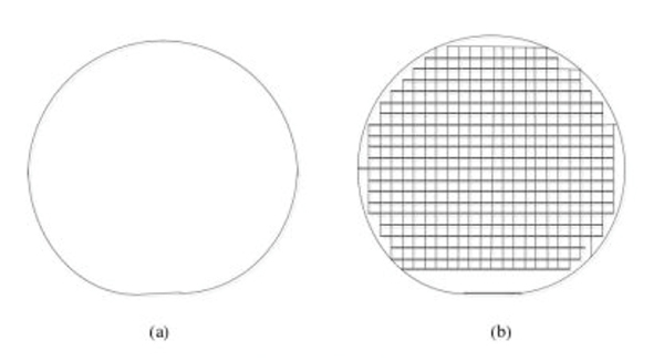
Figure 2 (a) Bare wafers (b) Patterned wafers
As shown in the figure above, wafers are divided into bare wafers and patterned wafers. There are many types of defects on the wafer surface, which may be produced in the process, or the defects of the material itself. Different defect detection methods can be used to classify the defects. Considering the physical properties of defects and the pertinence of defect detection algorithm, defects can be simply divided into surface redundancy (particles, pollutants, etc.), crystal defects (slip line defects, stacking faults), scratches, pattern defects (for patterned wafers).
Some crystal defects are caused by the changes in temperature, pressure and the medium components concentration during crystal growth; Some are caused by the thermal movement or stress of the particles after the crystal is formed. They can migrate and even disappear in the lattice; at the same time, new defects can be generated.